
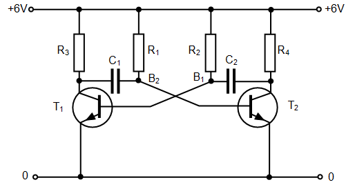
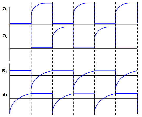
We will assume that transistor T1
is ON initially and transistor T2 is OFF.
When T1
is on O1 is at 0.2 V and B1 is at 0.7 V
T2 is off and
O2 is at 6 V and B2 is at ñ5.3 V
C1 charges up through R1
and C2 charges up through R4
As soon as B2 reaches 0.7 V T2 switches
on.
Note that C1 charges slowly through the large resistor R1 while C2
charges more quickly through the small resistor R4.
When T2 switches on
O2 drops to nearly 0 V, B1 drops by 6 V to ñ5.3 V and T1 goes
off. Both sides of C2 will drop by 6 V and it will take some time for C2 to adjust its charge, the
potential difference across it cannot change instantly.
The cycle now repeats for the
transistor.
The charge discharge rate and hence the switching action of the circuit
depends on C and R.