
If a
region of p-type material and a region of n-type material are formed side by side in a piece of
silicon, a p-n junction is formed. It is important that this is made in one piece of the material
so that the crystal lattice extends across the boundary. It is not sufficient just to have two
pieces in contact.
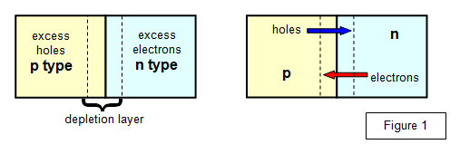
Both the p-type and the n-type material are electrically neutral, but
they both contain an imbalance of conduction electrons or holes. At the boundary, holes drift
from the p-type towards the n-type material and electrons drift from the n-type to the p-type
to reduce this imbalance. This diffusion of holes and electrons across the boundary sets up
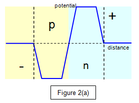
a potential barrier which prevents further change, the p-type region becoming slightly
negative and the n-type becoming slightly positive. The barrier has a potential difference
across it of about 0.1 V, although the exact size of the potential barrier depends on the
material. These effects only occur over a very small region (about 10-3 mm on
either side of the boundary) known as the depletion layer. They are summarised in Figure 1.
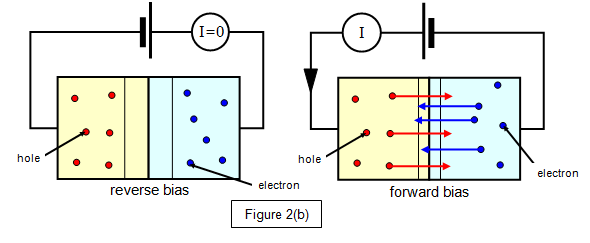
The p-n junction forms a semiconductor diode. If current is to flow through the
diode, then the latter must be connected in a circuit in such a way as to reduce the height of
the potential barrier, that is, the p-type material must be made positive to attract more
electrons and the n-type must be made negative.
Connecting it in such a way is
called forward bias, and round the other way is known as reverse bias. A reverse bias tends
to increase the width of the depletion layer while a forward bias will reduce the width of this
layer (see Figure 2).
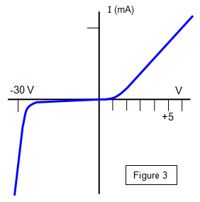
The characteristics of a germanium junction diode
are shown in Figure 3. When in the forward biased direction the current increases almost
linearly as the potential difference across it is increased, a potential difference of a volt
giving a current of a few milliamps. In the reverse direction the current is only a few
microamps until the diode breaks down, this occuring at a reverse potential difference of
some 30V.
Diodes must be protected from excess temperature, otherwise their
structure will be destroyed. The limit for germanium is about 100 oC, and that for silicon
about 200 oC.
Semiconductor diodes have several advantages over thermionic diode
valves. They are smaller, require less voltage to operate, do not waste so much energy as
heat and are quick and cheap to manufacture.