
In 1948 some work was carried out at the Bell Telephone
Laboratories in America that has changed our lives. This was the invention of the transistor
by Shockley, Brattain and Bardeen.
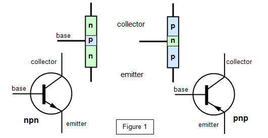
The transistor, basically a semiconductor triode,
consists of a thin central layer of one type of semiconductor between two relatively thick
pieces of the other type. The junction transistor can be of two types, as shown in Figure 1:
pnp or npn. The pnp transistor consists of a very thin piece of n-type material sandwiched
between two pieces of p-type, while the npn transistor has a central piece of p-type. The
pieces at either side are called the emitter and the collector while the central part is known
as the base. The base is lightly doped compared with the emitter and the collector, and is
only about 3-5 μm thick.
From now on we will consider only the npn transistor as it
is now in more common use in schools. The npn silicon transistor is connected into the
circuit as shown by Figure 2. The emitter-base junction is forward biased and the base-
collector junction is reverse biased.
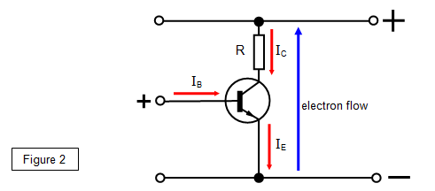
The
collector current (IC) is usually over 99% of IE and
IB is less than 1 per cent.
The name 'transistor' comes from the words
'transfer of resistance': the emitter-base junction is forward biased and therefore has a low
resistance, while the base-collector is reverse biased and has a high resistance.
The properties of the transistor described above lead us to consider it as a
current amplifier.
For its basic operation, the circuit is set up as shown in Figure 4, and the value of R is chosen so that the transistor is switched on, that is, the potential at the base is at least 0.6 V.
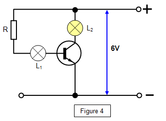
Lamp L2 lights but
L1 does not, showing that the collector current must be much larger than the base
current.
If L1 is removed, however, L2 goes out because no potential is being
applied to the base.
A transistor will not conduct (that is, no current will flow through from the
collector to the emitter) unless there is a also potential difference between the emitter and
the base of at least 0.6 V. This property enables the transistor to be used as a switch: it is
'on' when the base-emitter potential difference is bigger than 0.6 V and 'off' when it
isn't.
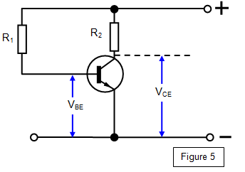
If you consider the circuit in Figure
5, then when the transistor is off, that is, there is no current flowing through it, the potential
difference across the emitter-collector (VCE) is high. As soon as the transistor
starts to conduct this potential difference falls to very close to zero (Figure 6).
 Therefore
the output potential difference (VCE) is small when the input potential difference
(VBE) is large, and large when the input potential difference is small, that is less
than 0.6 V.
This is the basic NOT logic gate circuit. (see the section on Logic gates in the Foundation level for a further treatment).
Therefore
the output potential difference (VCE) is small when the input potential difference
(VBE) is large, and large when the input potential difference is small, that is less
than 0.6 V.
This is the basic NOT logic gate circuit. (see the section on Logic gates in the Foundation level for a further treatment).
We will now consider two circuits in which the switching action of a transistor is important.

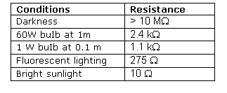
The circuit includes a light-dependent resistor (LDR), the resistance of which changes with illumination. A table showing the variation for a light-dependent resistor in common use is shown below.
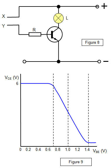
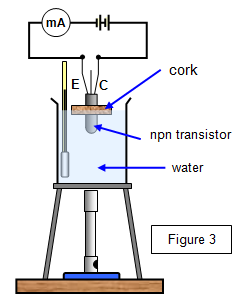
The circuit is shown in Figure 8. If the base circuit is broken at XY then the transistor is off, but if the probes XY are placed in a conducting liquid the transistor switches on. This could be used as a liquid level indicator for a blind person, the lamp L being replaced by a buzzer and the two contacts being placed at a suitable level in a cup or bowl.
We have
seen that when VBE >0.6 V the transistor switches on, and Figure 9 shows that as
VBE is increased above this value VCE falls and reaches a steady value
(close to zero) when VBE is about 1.4 V. Any further increase in VBE
does not change VCE.
In this condition the transistor is said to have
bottomed or be saturated.